
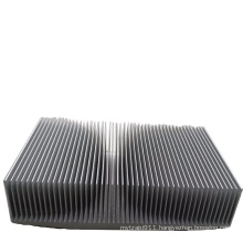
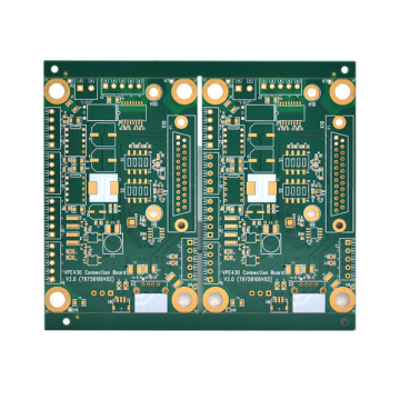
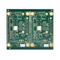
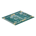
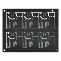
face recognition attendance Heavy copper board
Basic Info
Model No.: Thick Copper PCBA
Product Description
What is heavy copper PCB?
In the case of complex key PCB layout requirements, electronics manufacturers and PCB manufacturers also have the same attention to reliable, high-quality, and low-cost electronic solutions. A recent growth trend in PCB manufacturing is the use of heavy copper in PCB manufacturing. This article reveals the richness of the use of heavy copper in printed circuit board manufacturing. In addition, it also provides technical details on the use of heavy copper substrates to manufacture PCBs.
The structure of the printed circuit board made of heavy copper uses a fine combination of copper electroplating and copper etching. As thin copper foil, these layers are made with circuits. In addition, copper etching technology makes it possible to eliminate unnecessary copper and copper electroplating techniques, thereby optimizing the copper thickness of traces, pads, planes, and holes on the circuit board. The epoxy-based substrate is used to complete the final lamination of the middle layer of the circuit board. These heavy copper PCBs are made of thermal layers and are most suitable for multilayer PCB structures. In short, thick copper PCBs are manufactured using a large amount of finished copper in the internal and external substrates of the circuit board, also known as laminate deposition.
Heavy copper board is most suitable for compact electronic solutions because it can remove or allocate minimal space for cooling fans or radiators, thus taking up less space.
High current carrying capacity.
High temperature resistance.
The use of heavy copper base material has high durability.
Easily transfer heat to the external heat sink.
High quality, repetitive resistance can destroy the thermal cycle of normal PCB in a few seconds.
Very feasible in harsh environments.
It has high resistance to thermal strain.
Using the perfect combination of electroplating technology and copper etching technology, negligible undercuts and straight side walls are obtained.
Characteristic impedance PCB is proven to be rough, tough, and low in power distribution impedance.
The heavy copper in the circuit board can also be connected to standard circuits.
Using heavy copper electroplating technology can produce large current circuits, which is helpful to observe the simple and dense beard structure.
Highly reliable electronic performance is achieved by using heavy copper PCB layout or extreme copper PCB.
The use of heavy copper in PCB manufacturing can reduce the board area and reduce the number of layers on the circuit board.
Increase the mechanical strength of the plating layer and the position of the connector.
It is possible that you will not have special materials that repeat the copper PCB layout under high temperature conditions.
Another main reason for the high usage rate of heavy copper PCB is Cable Connectors I/O Connectors configuration. Relying on these abundant heavy copper PCBs, researchers are moving towards effective methods to implement unique PCB layouts to meet complex requirements, making their low cost pcb manufacturing benefits, and at the same time providing high High Quality Prototype PCB Fabrication.


Product Categories : High Frequency Board > HDI PCB